-
Categories
-
 NS Series Kit
-
 Arduino, ESP, Raspberry Pi ETC
-
 Arduino Accessories
- Others
- Gyroscope And Accelerometer Sensor
- Recording Module
- Wheel
- Fingerprint Reader
- Car Chassis And Wheel
- Valve And Lock
- Converter
- Buzzer Module
- Rotary Encoder Module
- Bluetooth Module
- Timer Module
- Joy Stick And Key Pad Module
- Micro SD Card Module
- Relay Module
- nRF | GSM And GPS
- Digital Multiplexer
- Motor
- Arduino Shield
- Display
-
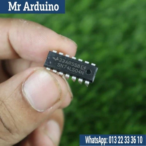
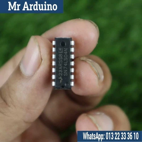
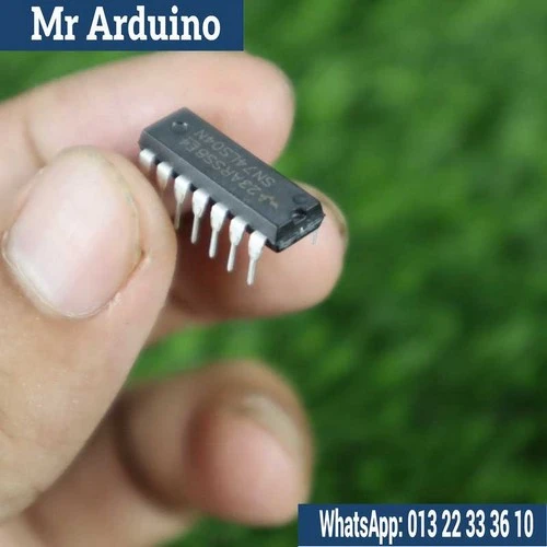
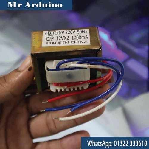
 Electronics Component
-
 Sensor & Sensor Module
-
 Drone | Plane | RC Parts
-
 Multimeter And Measurement
-
 Industrial Items
-
 IPS
IPS
-